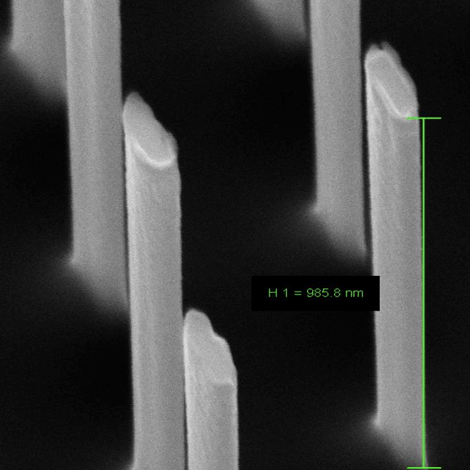
MetaPhoX manufactures high-performance flat focusing optics based on engineered dielectric metasurfaces (metalenses) fabricated on 1-inch silicon wafers. Specifically designed for Near-Infrared (NIR) operation, these optical components are realized using high-resolution nanofabrication processes capable of producing controlled subwavelength structures over wafer-scale substrates. The MetaPhoX platform supports both standard product configurations and custom-designed focusing optics tailored to specific application requirements, including wavelength, focal length, numerical aperture, and aperture diameter.
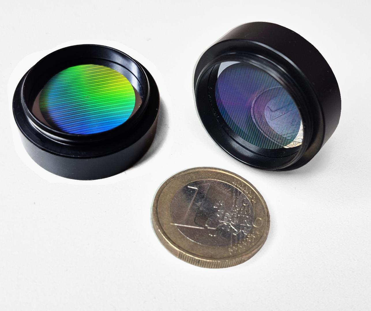
Standard products
MetaPhoX currently offers standard silicon dielectric focusing lenses with the following specifications:
| Substrate Diameter | 1 inch (2.54 cm) |
| Clear aperture | 20 mm |
| Substrate material | Silicon, ARC on the back |
| Operating wavelength | 1310 nm, 1550 nm |
| Zero order intensity | <3% |
| Focal lengths (in mm) | 15, 20, 25, 30, 35, 40, 50, 75, 100, 200, 500, 1000, 2000 |
| Fabrication | EBL + Nanoimprinting |
| Packaging | Bare wafer or mounted |
Custom products
Custom focusing metalenses can be designed according to customer specifications, including:
| Operating wavelength | from 1200 nm to 1700 nm |
| Clear aperture | Customizable, 20 mm |
| Focal length | Custom, numerical aperture |
| Polarization engineering | Custom |
If larger lenses are needed, please check our large metalenses section.
MetaPhoX Technology Platform
MetaPhoX metalenses are enabled by a proprietary design and fabrication platform that combines advanced electromagnetic design with state-of-the-art nanofabrication technologies. Each optical component consists of millions of dielectric nano-pillars engineered to locally control the optical wavefront with subwavelength precision, enabling diffraction-limited focusing in an ultra-thin planar architecture.
The fabrication process begins with high-resolution Electron Beam Lithography (EBL), used to generate master patterns featuring 50 nm critical dimensions and high-aspect-ratio dielectric nanostructures. These masters are subsequently replicated using Nanoimprint Lithography (NIL), providing a scalable manufacturing route for high-volume production while preserving nanometer-scale accuracy.
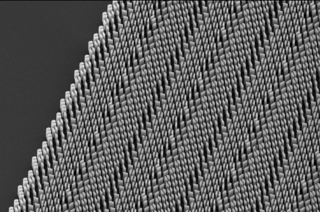
The MetaPhoX technology platform offers:
- High aspect-ratio dielectric meta-atoms (AR > 18)
- 50 nm critical dimension control
- Excellent profile verticality and dimensional uniformity
- Wafer-scale fabrication
- High diffraction efficiency and negligible zero-order leakage
- Compatibility with custom metasurface designs, high-NA optics and multifunctional optical components
The combination of advanced nanofabrication, rigorous electromagnetic design, and scalable replication technologies enables the realization of large-area flat optics combining high optical efficiency, excellent wavefront quality, and industrial manufacturability.